.jpg?format=webp)
Exploring the Complexities of PCIe Connectivity and Peer-to-Peer Communication
In this post we will take an in-depth look at communication bottlenecks within the PCIe bus and how some of Exxact's latest systems are designed to push the boundaries of intranode communication with wide reaching benefits for GPU heavy fields such as Machine Learning and Life Sciences Research.
The Traditional Approach
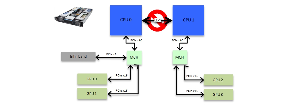
Before discussing the pros and cons of different types of PCIe bus layouts it is first necessary to understand why the speed of communication over the PCIe bus has become so important. Until the GPU computing revolution, that began in earnest in 2007, the PCI bus was typically only used for communicating to and from disk or through interconnects such as infiniband to other nodes. The information being written to disk, or communicated, resided in the DRAM attached to the CPUs and as such communication was typically from the DRAM, through the CPU onto the PCI bus via a memory controller hub (MCH) and then to the relevant device. A typical PCIe bus layout for such a node is shown in figure 1.
When it comes to GPU computing, where it is essential to be able to send data between individual GPUs as fast as possible, there are three major issues with this traditional design.
The first is that the GPUs are split into two domains on separate memory controller hubs attached to different CPU sockets. The nature of the QPI link connecting the two CPUs is such that a direct P2P copy between GPU memory is not possible if the GPUs reside on different PCIe domains. Thus a copy from the memory of GPU 0 to the memory of GPU 2 requires first copying over the PCIe link to the memory attached to CPU 0, then transferring over the QPI link to CPU 1 and over the PCIe again to GPU 2. As you can imagine this process adds a significant amount of overhead in both latency and bandwidth terms.
The second is that the number of PCIe channels available is limited to the number of channels provided by the CPU. In the case of current generation Intel Haswell CPUs, such as the E5-26XXv3 series, this is limited to 40 channels. In a dual socket system one is thus limited to a maximum of 4 GPUs in a single node, and in a single socket system just two GPUs, if they are all to have full x16 PCIe bandwidth. To utilize more GPUs at once requires a multi-node configuration employing expensive, and compared to PCIe P2P communication, relatively slow interconnects such as infiniband. Even then the number of spare PCIe channels limits the interconnect bandwidth that can be deployed and in the example above leads to undesirable heterogeneity and bottlenecks in terms of the efficiency with which different GPUs can communicate over the internode link. GPU 2 and 3 for example have to go through the CPU in order to communicate over the infiniband link.
The third issue is that even for the pairs of GPUs that can communicate directly via P2P copies the nature of the MCH is such that it prevents the full PCIe bandwidth from being fully utilized.
The PCIe topology of a node, and the bandwidth limitations, can be investigated further by using two tools that ship with the NVIDIA driver and CUDA toolkit. The first is the command nvidia-smi that can be used to display the PCIe topology:
nvidia-smi topo -m
GPU0 GPU1 GPU2 GPU3 CPU Affinity
GPU0 X PHB SOC SOC 0-9,20-29
GPU1 PHB X SOC SOC 0-9,20-29
GPU2 SOC SOC X PHB 10-19,30-39
GPU3 SOC SOC PHB X 10-19,30-39
Legend:
X = Self
SOC = Path traverses a socket-level link (e.g. QPI)
PHB = Path traverses a PCIe host bridge
PXB = Path traverses multiple PCIe internal switches
PIX = Path traverses a PCIe internal switch
This table shows us what figure 1 above illustrates graphically, that the GPUs are in pairs, 0 & 1 and 2 & 3 and connected via the PCIe host bridge. Using the p2pBandwidthLatencyTest that ships with the NVIDIA CUDA Samples we can easily illustrate the bottlenecks that such a traditional PCIe topology introduces.
p2pBandwidthLatencyTest
Bidirectional P2P=Enabled Bandwidth Matrix (GB/s)
D\D 0 1 2 3
0 X 19.18 12.22 11.77
1 19.17 X 17.07 11.81
2 12.23 12.17 X 19.17
3 11.73 11.88 19.18 X
The difference in communication bandwidth when the QPI connection is involved is immediately apparent, ~12GB/s vs ~19GB/s. What is not so obvious though, but will be clearer when we look at alternative motherboard designs below, is that, because of the PCIe host bridge involvement, the achievable bidirectional bandwidth even in the P2P case is substantially less than the theoretical maximum x16 PCIe Gen 3.0 limit of 32 GB/s. This communication bottleneck also appears in the communication latency between GPUs, also shown by the p2pBandwidthLatencyTest tool.
P2P=Enabled Latency Matrix (us)
D\D 0 1 2 3
0 3.39 8.18 16.86 16.26
1 7.22 3.74 13.56 16.54
2 16.27 16.06 3.52 5.81
3 15.98 15.92 6.62 3.20
Here it is immediately obvious that the communication latency between GPUs on different PCIe domains is substantially higher than those that can communicate via P2P.
Rethinking Motherboard Design in a GPU Centric Fashion
The net result of these issues is that, while often cost effective, the traditional design of the PCIe bus on single and multisocket motherboards is not well suited for modern multi-GPU accelerated software. Fortunately the design of PCIe is such that one is not constrained by this traditional CPU centric approach to motherboard design and with the use of PCIe (PLX) switch chips (Figure 2), which currently exist in 48, 80 and 96 channel designs, it is possible to design motherboards that are GPU centric and maximize intranode GPU to GPU communication potential while remaining extremely cost effective. This approach is what Exxact have done in their range of GPU optimum workstation and server designs. In the sections that follow we will review each of the different designs available and highlight the pros and cons of each.

Figure 2: 48 channel PLC Technology PCIe switch chip.
Design 1: Deep Learning Dev Box
The Spectrum TXN003-0128N, better known as the Deep Learning Dev Box was first offered by Exxact in January 2014 and the design was subsequently used as the basis for NVIDIA's Digits Dev Box (https://developer.nvidia.com/devbox). This system is designed to provide an optimum balance between PCIe communication speed over 4 GPUs and price in a desktop form factor. The PCIe topology of this system is based on coupling two 8747 PLX switches together to allow 4 GPUs to be hosted, each at full x16 bandwidth, in a single CPU socket system while at the same time providing P2P communication support between all 4 GPUs. The PCIe topology is shown in Figure 3 below.
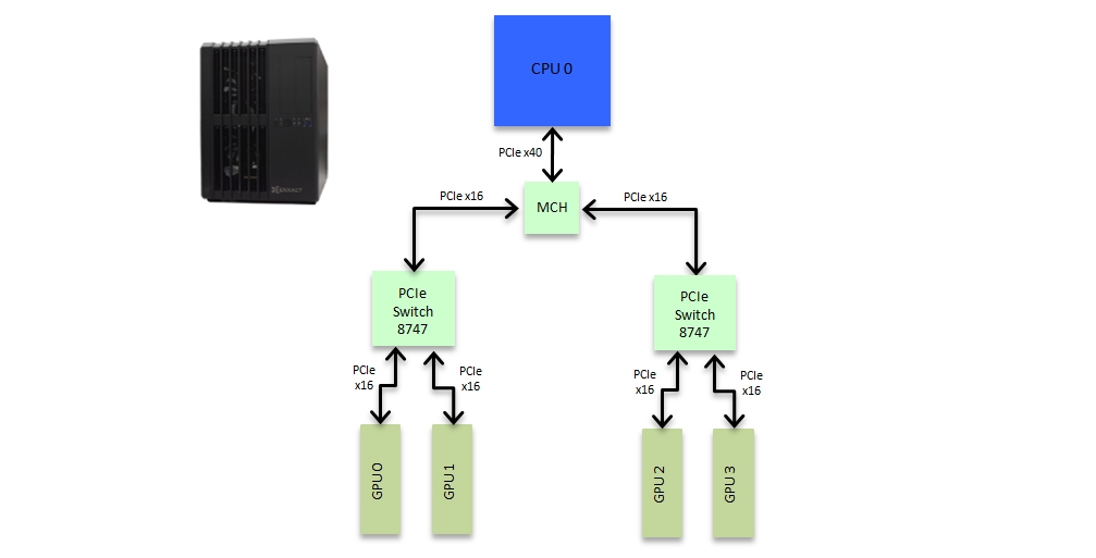
Figure 2: Exxact Deep Learning Dev Box PCIe topology
Unlike the traditional design the use of the two cost effective 8747 PLX switches allows the 4 GPUs to be hosted in the same PCIe domain and for the system to only require a single CPU socket. This is what allows Exxact to offer this complete system, with a full Deep Learning Software stack for just $8999. P2P communication is possible between all 4 GPUs here although there is still an x16 bottleneck (and the MCH) between the two banks of GPUs. However as can be seen from the p2pBandwidthLatencyTest result the communication performance between the 4 GPUs is much improved over the traditional motherboard design.
nvidia-smi topo -m
GPU0 GPU1 GPU2 GPU3 CPU Affinity
GPU0 X PIX PHB PHB 0-11
GPU1 PIX X PHB PHB 0-11
GPU2 PHB PHB X PIX 0-11
GPU3 PHB PHB PIX X 0-11
Legend:
X = Self
SOC = Path traverses a socket-level link (e.g. QPI)
PHB = Path traverses a PCIe host bridge
Bidirectional P2P=Enabled Bandwidth Matrix (GB/s)
D\D 0 1 2 3
0 X 26.13 20.31 20.32
1 25.97 X 20.31 20.32
2 20.32 20.32 X 26.12
3 20.32 20.32 26.12 X
Not only has the bandwidth between GPU pairs 0 & 1 and 2 & 3 improved significantly, getting much closer to the 32GB/s theoretical maximum, due to the replacement of the MCH connection with a direct PLX switch, so has the bandwidth between the two GPU groups although there is still a drop due to the MCH and the fact that ultimately all to all communication would need to share the single x16 connection between the two GPU banks. Nevertheless this provides a very cost effective but high performance GPU centric workstation. The design also greatly improves the communication latency.
P2P=Enabled Latency Matrix (us)
D\D 0 1 2 3
0 4.15 6.10 6.27 6.05
1 6.10 4.13 6.12 6.00
2 6.31 5.96 4.19 6.04
3 6.07 5.97 6.15 4.09
Comparing this with the traditional design above we can see in the worst case the latency between any GPUs is at most 6.31 microseconds. This is a substantial improvement over the 16.86 microseconds in the traditional design. Hence the reason this design is so effective as a workstation for machine learning applications.
Design 2: A Cost Effective 8 GPU System
Often having 4 GPUs in a single node is not enough horsepower. Of course one can always connect nodes together using high speed interconnects but this is both expensive and a substantial communication bottleneck. A solution to this is Exxact's Tensor TXR430-1500R 8 GPU system.
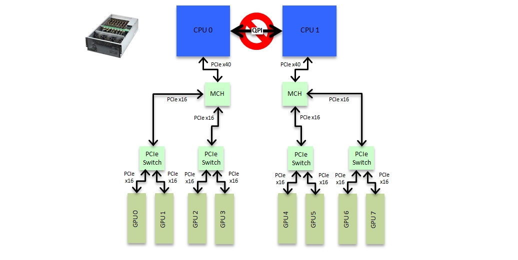
Figure 3: Low cost 8 GPU box design
This effectively gives two Deep Learning Dev Boxes in the same node. The topology for each bank of 4 GPUs is the same as the Dev Box above. The design has the obvious restriction that P2P communication is not possible between the two banks of 4 GPUs, as can be seen in the bandwidth numbers below, but the use of cost effective 8747 PLX switches makes this a very cost effective node design. Indeed since there are savings on only needing a single case, a single disk system, single set of CPU memory DIMMS etc this 8 way system can actually come out cheaper than two separate Deep Learning Dev Boxes while at the same time providing the flexibility of having 8 GPUs available in a single node.
GPU0 GPU1 GPU2 GPU3 GPU4 GPU5 GPU6 GPU7 CPU Affinity
GPU0 X PIX PHB PHB SOC SOC SOC SOC 0-7,16-23
GPU1 PIX X PHB PHB SOC SOC SOC SOC 0-7,16-23
GPU2 PHB PHB X PIX SOC SOC SOC SOC 0-7,16-23
GPU3 PHB PHB PIX X SOC SOC SOC SOC 0-7,16-23
GPU4 SOC SOC SOC SOC X PIX PHB PHB 8-15,24-31
GPU5 SOC SOC SOC SOC PIX X PHB PHB 8-15,24-31
GPU6 SOC SOC SOC SOC PHB PHB X PIX 8-15,24-31
GPU7 SOC SOC SOC SOC PHB PHB PIX X 8-15,24-31
Legend:
X = Self
SOC = Path traverses a socket-level link (e.g. QPI)
PHB = Path traverses a PCIe host bridge
PIX = Path traverses a PCIe internal switch
Bidirectional P2P=Enabled Bandwidth Matrix (GB/s)
D\D 0 1 2 3 4 5 6 7
0 X 24.91 18.22 19.38 14.20 12.36 8.83 11.05
1 25.27 X 19.63 19.63 9.95 15.24 13.50 14.74
2 19.63 19.61 X 25.27 11.96 16.11 13.73 15.18
3 19.63 19.62 25.30 X 13.87 16.76 13.68 15.69
4 15.20 9.93 11.93 13.83 X 25.30 19.63 19.62
5 12.59 15.41 16.19 17.12 25.28 X 19.62 19.63
6 9.29 13.52 13.55 13.61 19.68 19.67 X 25.30
7 11.10 15.11 15.16 15.60 19.67 19.67 25.31 X
Design 3: Full 8 GPU P2P Support
As mentioned above there are currently three versions of the PLX PCIe switch, the 48 channel, 80 channel and 96 channel versions. Designs 1 and 2 above make use of the cost effective 48 channel switches however if one changes to using the higher channel count switches it is possible, within certain distance limits imposed by the requirements of PCIe, to build systems with very high bandwidth system-wide PCIe peer to peer support. Exxact offers two such designs, one supporting up to 8 GPUs and the second up to an astounding 20 GPUs. The 8 GPU system (Tensor TXR550-512R) design is as follows.
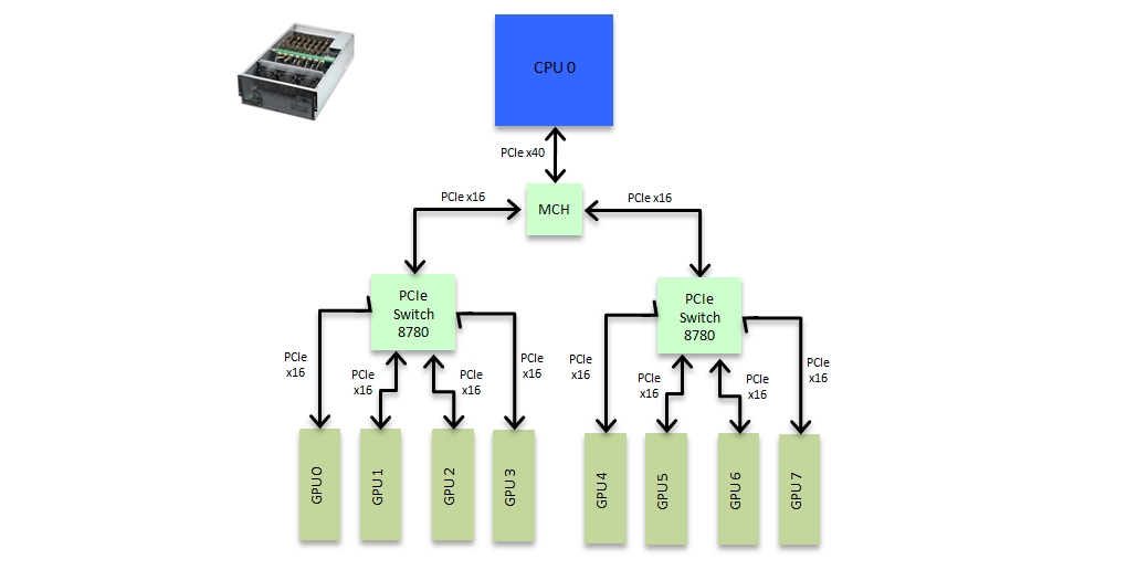
Figure 4: Full 8 way P2P GPU box design
This was the first system to offer peer-to-peer support across 8 GPUs although it should be obvious from figure 4 that it introduces an unfortunate bottleneck between the two banks of 4 GPUs. Firstly all 4 GPUs on a given PCIe switch have to share a single x16 link to the other bank of 4 GPUs but in addition communication is unfortunately slowed by having to go through the MCH. This can be seen in the bandwidth breakdown.
Tensor TXR550-512R
nvidia-smi topo -m
GPU0 GPU1 GPU2 GPU3 GPU4 GPU5 GPU6 GPU7 CPU Affinity
GPU0 X PIX PIX PIX PHB PHB PHB PHB 0-11
GPU1 PIX X PIX PIX PHB PHB PHB PHB 0-11
GPU2 PIX PIX X PIX PHB PHB PHB PHB 0-11
GPU3 PIX PIX PIX X PHB PHB PHB PHB 0-11
GPU4 PHB PHB PHB PHB X PIX PIX PIX 0-11
GPU5 PHB PHB PHB PHB PIX X PIX PIX 0-11
GPU6 PHB PHB PHB PHB PIX PIX X PIX 0-11
GPU7 PHB PHB PHB PHB PIX PIX PIX X 0-11
Legend:
X = Self
PHB = Path traverses a PCIe host bridge
PIX = Path traverses a PCIe internal switch
Bidirectional P2P=Enabled Bandwidth Matrix (GB/s)
D\D 0 1 2 3 4 5 6 7
0 X 25.03 25.02 25.02 15.96 15.96 14.73 15.97
1 25.02 X 25.03 25.02 15.97 15.97 14.73 15.97
2 25.03 25.01 X 25.04 15.97 15.97 14.73 15.97
3 25.04 25.02 25.04 X 14.69 14.69 14.70 14.70
4 16.00 16.00 16.00 14.73 X 25.02 25.03 25.02
5 16.00 16.01 16.00 14.73 25.01 X 25.04 25.04
6 14.69 14.69 14.70 14.70 25.02 25.04 X 25.02
7 16.01 16.01 16.00 14.73 25.02 25.02 25.02 X
As is evident from this table while the bandwidth within each bank of 4 GPUs is close to the theoretical maximum between the banks it gets cut considerably. The latency is affected in a similar way. As such while this design was novel in being the first to support P2P across 8 GPUs it is not ideal. It is for this reason that this design has now been superseded by what is arguably the most capable GPU computing solution currently available.
Design 4: Taking GPU computing to 11 - Exxact's extreme 20 way P2P GPU monster
Having learnt from previous designs Exxact now offer the Tensor TXR414-1000R system. This system takes GPU computing to 11 offering an incredible 140 TFlops of computing capacity in a single 4U chassis. This equates to 1.4 PFlops in a single rack. It takes the concept of PCIe P2P communication to the limit supporting full P2P communication across up to 20 GPUs. This system can incorporate 10 standard Titan-X or M40 GPUs or, with modified single width high performance heatsinks, 20 single wide Titan-X or M40 GPUs in a single system image. It makes use of the top of the line 96 channel PLX switches in a topology that ensures no GPU to GPU communication is slowed by needing to traverse the MCH. It is truly a supercomputer in a single node with a PCIe topology that in itself could be considered a work of art.
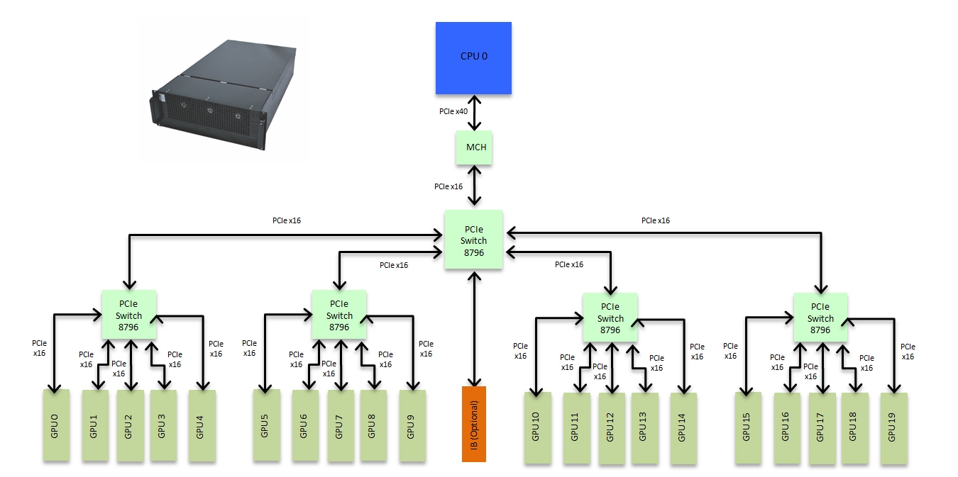
Figure 5: 20 way P2P GPU box design
This system is available for shipping and represents the current state of the art in GPU computing. It is the perfect tool for anyone in the machine-learning environment looking to push the boundaries of performance for multi-GPU software and the design is such that it remains future proofed when it comes to Pascal and NVLink. The benefit of this design is obvious when looking at the bandwidth offered between GPUs.
Bidirectional P2P=Enabled Bandwidth Matrix (GB/s)
D\D 0 1 2 3 4 5 6 7 8 9
0 X 24.95 24.96 24.95 24.96 24.95 24.94 24.96 24.95 24.96
1 24.96 X 24.98 24.95 24.95 24.95 24.95 24.96 24.95 24.97
2 24.98 24.97 X 24.96 24.96 24.97 24.95 24.96 24.97 24.97
3 24.97 24.96 24.95 X 24.97 24.96 24.94 24.96 24.96 24.96
4 24.95 24.94 24.96 24.97 X 24.95 24.94 24.95 24.96 24.93
5 24.96 24.95 24.97 24.95 24.96 X 24.94 24.95 24.96 24.95
6 24.96 24.95 24.95 24.96 24.95 24.96 X 24.96 24.96 24.93
7 24.96 24.95 24.96 24.96 24.95 24.95 24.93 X 24.97 24.93
8 24.97 24.95 24.96 24.96 24.95 24.97 24.95 24.96 X 24.96
9 24.96 24.96 24.95 24.95 24.96 24.97 24.94 24.97 24.93 X
Not only is the bandwidth close to the theoretical maximum it is also highly consistent across all GPUs. This system should thus be seriously considered by anyone using or developing multi-GPU P2P enabled machine-learning software.
Find out more about NVIDIA Tesla P2P technology and our latest solutions.
.jpg?format=webp)
Exploring the Complexities of PCIe Connectivity and Peer-to-Peer Communication
Exploring the Complexities of PCIe Connectivity and Peer-to-Peer Communication
In this post we will take an in-depth look at communication bottlenecks within the PCIe bus and how some of Exxact's latest systems are designed to push the boundaries of intranode communication with wide reaching benefits for GPU heavy fields such as Machine Learning and Life Sciences Research.
The Traditional Approach
Before discussing the pros and cons of different types of PCIe bus layouts it is first necessary to understand why the speed of communication over the PCIe bus has become so important. Until the GPU computing revolution, that began in earnest in 2007, the PCI bus was typically only used for communicating to and from disk or through interconnects such as infiniband to other nodes. The information being written to disk, or communicated, resided in the DRAM attached to the CPUs and as such communication was typically from the DRAM, through the CPU onto the PCI bus via a memory controller hub (MCH) and then to the relevant device. A typical PCIe bus layout for such a node is shown in figure 1.

When it comes to GPU computing, where it is essential to be able to send data between individual GPUs as fast as possible, there are three major issues with this traditional design.
The first is that the GPUs are split into two domains on separate memory controller hubs attached to different CPU sockets. The nature of the QPI link connecting the two CPUs is such that a direct P2P copy between GPU memory is not possible if the GPUs reside on different PCIe domains. Thus a copy from the memory of GPU 0 to the memory of GPU 2 requires first copying over the PCIe link to the memory attached to CPU 0, then transferring over the QPI link to CPU 1 and over the PCIe again to GPU 2. As you can imagine this process adds a significant amount of overhead in both latency and bandwidth terms.
The second is that the number of PCIe channels available is limited to the number of channels provided by the CPU. In the case of current generation Intel Haswell CPUs, such as the E5-26XXv3 series, this is limited to 40 channels. In a dual socket system one is thus limited to a maximum of 4 GPUs in a single node, and in a single socket system just two GPUs, if they are all to have full x16 PCIe bandwidth. To utilize more GPUs at once requires a multi-node configuration employing expensive, and compared to PCIe P2P communication, relatively slow interconnects such as infiniband. Even then the number of spare PCIe channels limits the interconnect bandwidth that can be deployed and in the example above leads to undesirable heterogeneity and bottlenecks in terms of the efficiency with which different GPUs can communicate over the internode link. GPU 2 and 3 for example have to go through the CPU in order to communicate over the infiniband link.
The third issue is that even for the pairs of GPUs that can communicate directly via P2P copies the nature of the MCH is such that it prevents the full PCIe bandwidth from being fully utilized.
The PCIe topology of a node, and the bandwidth limitations, can be investigated further by using two tools that ship with the NVIDIA driver and CUDA toolkit. The first is the command nvidia-smi that can be used to display the PCIe topology:
nvidia-smi topo -m
GPU0 GPU1 GPU2 GPU3 CPU Affinity
GPU0 X PHB SOC SOC 0-9,20-29
GPU1 PHB X SOC SOC 0-9,20-29
GPU2 SOC SOC X PHB 10-19,30-39
GPU3 SOC SOC PHB X 10-19,30-39
Legend:
X = Self
SOC = Path traverses a socket-level link (e.g. QPI)
PHB = Path traverses a PCIe host bridge
PXB = Path traverses multiple PCIe internal switches
PIX = Path traverses a PCIe internal switch
This table shows us what figure 1 above illustrates graphically, that the GPUs are in pairs, 0 & 1 and 2 & 3 and connected via the PCIe host bridge. Using the p2pBandwidthLatencyTest that ships with the NVIDIA CUDA Samples we can easily illustrate the bottlenecks that such a traditional PCIe topology introduces.
p2pBandwidthLatencyTest
Bidirectional P2P=Enabled Bandwidth Matrix (GB/s)
D\D 0 1 2 3
0 X 19.18 12.22 11.77
1 19.17 X 17.07 11.81
2 12.23 12.17 X 19.17
3 11.73 11.88 19.18 X
The difference in communication bandwidth when the QPI connection is involved is immediately apparent, ~12GB/s vs ~19GB/s. What is not so obvious though, but will be clearer when we look at alternative motherboard designs below, is that, because of the PCIe host bridge involvement, the achievable bidirectional bandwidth even in the P2P case is substantially less than the theoretical maximum x16 PCIe Gen 3.0 limit of 32 GB/s. This communication bottleneck also appears in the communication latency between GPUs, also shown by the p2pBandwidthLatencyTest tool.
P2P=Enabled Latency Matrix (us)
D\D 0 1 2 3
0 3.39 8.18 16.86 16.26
1 7.22 3.74 13.56 16.54
2 16.27 16.06 3.52 5.81
3 15.98 15.92 6.62 3.20
Here it is immediately obvious that the communication latency between GPUs on different PCIe domains is substantially higher than those that can communicate via P2P.
Rethinking Motherboard Design in a GPU Centric Fashion
The net result of these issues is that, while often cost effective, the traditional design of the PCIe bus on single and multisocket motherboards is not well suited for modern multi-GPU accelerated software. Fortunately the design of PCIe is such that one is not constrained by this traditional CPU centric approach to motherboard design and with the use of PCIe (PLX) switch chips (Figure 2), which currently exist in 48, 80 and 96 channel designs, it is possible to design motherboards that are GPU centric and maximize intranode GPU to GPU communication potential while remaining extremely cost effective. This approach is what Exxact have done in their range of GPU optimum workstation and server designs. In the sections that follow we will review each of the different designs available and highlight the pros and cons of each.

Figure 2: 48 channel PLC Technology PCIe switch chip.
Design 1: Deep Learning Dev Box
The Spectrum TXN003-0128N, better known as the Deep Learning Dev Box was first offered by Exxact in January 2014 and the design was subsequently used as the basis for NVIDIA's Digits Dev Box (https://developer.nvidia.com/devbox). This system is designed to provide an optimum balance between PCIe communication speed over 4 GPUs and price in a desktop form factor. The PCIe topology of this system is based on coupling two 8747 PLX switches together to allow 4 GPUs to be hosted, each at full x16 bandwidth, in a single CPU socket system while at the same time providing P2P communication support between all 4 GPUs. The PCIe topology is shown in Figure 3 below.

Figure 2: Exxact Deep Learning Dev Box PCIe topology
Unlike the traditional design the use of the two cost effective 8747 PLX switches allows the 4 GPUs to be hosted in the same PCIe domain and for the system to only require a single CPU socket. This is what allows Exxact to offer this complete system, with a full Deep Learning Software stack for just $8999. P2P communication is possible between all 4 GPUs here although there is still an x16 bottleneck (and the MCH) between the two banks of GPUs. However as can be seen from the p2pBandwidthLatencyTest result the communication performance between the 4 GPUs is much improved over the traditional motherboard design.
nvidia-smi topo -m
GPU0 GPU1 GPU2 GPU3 CPU Affinity
GPU0 X PIX PHB PHB 0-11
GPU1 PIX X PHB PHB 0-11
GPU2 PHB PHB X PIX 0-11
GPU3 PHB PHB PIX X 0-11
Legend:
X = Self
SOC = Path traverses a socket-level link (e.g. QPI)
PHB = Path traverses a PCIe host bridge
Bidirectional P2P=Enabled Bandwidth Matrix (GB/s)
D\D 0 1 2 3
0 X 26.13 20.31 20.32
1 25.97 X 20.31 20.32
2 20.32 20.32 X 26.12
3 20.32 20.32 26.12 X
Not only has the bandwidth between GPU pairs 0 & 1 and 2 & 3 improved significantly, getting much closer to the 32GB/s theoretical maximum, due to the replacement of the MCH connection with a direct PLX switch, so has the bandwidth between the two GPU groups although there is still a drop due to the MCH and the fact that ultimately all to all communication would need to share the single x16 connection between the two GPU banks. Nevertheless this provides a very cost effective but high performance GPU centric workstation. The design also greatly improves the communication latency.
P2P=Enabled Latency Matrix (us)
D\D 0 1 2 3
0 4.15 6.10 6.27 6.05
1 6.10 4.13 6.12 6.00
2 6.31 5.96 4.19 6.04
3 6.07 5.97 6.15 4.09
Comparing this with the traditional design above we can see in the worst case the latency between any GPUs is at most 6.31 microseconds. This is a substantial improvement over the 16.86 microseconds in the traditional design. Hence the reason this design is so effective as a workstation for machine learning applications.
Design 2: A Cost Effective 8 GPU System
Often having 4 GPUs in a single node is not enough horsepower. Of course one can always connect nodes together using high speed interconnects but this is both expensive and a substantial communication bottleneck. A solution to this is Exxact's Tensor TXR430-1500R 8 GPU system.

Figure 3: Low cost 8 GPU box design
This effectively gives two Deep Learning Dev Boxes in the same node. The topology for each bank of 4 GPUs is the same as the Dev Box above. The design has the obvious restriction that P2P communication is not possible between the two banks of 4 GPUs, as can be seen in the bandwidth numbers below, but the use of cost effective 8747 PLX switches makes this a very cost effective node design. Indeed since there are savings on only needing a single case, a single disk system, single set of CPU memory DIMMS etc this 8 way system can actually come out cheaper than two separate Deep Learning Dev Boxes while at the same time providing the flexibility of having 8 GPUs available in a single node.
GPU0 GPU1 GPU2 GPU3 GPU4 GPU5 GPU6 GPU7 CPU Affinity
GPU0 X PIX PHB PHB SOC SOC SOC SOC 0-7,16-23
GPU1 PIX X PHB PHB SOC SOC SOC SOC 0-7,16-23
GPU2 PHB PHB X PIX SOC SOC SOC SOC 0-7,16-23
GPU3 PHB PHB PIX X SOC SOC SOC SOC 0-7,16-23
GPU4 SOC SOC SOC SOC X PIX PHB PHB 8-15,24-31
GPU5 SOC SOC SOC SOC PIX X PHB PHB 8-15,24-31
GPU6 SOC SOC SOC SOC PHB PHB X PIX 8-15,24-31
GPU7 SOC SOC SOC SOC PHB PHB PIX X 8-15,24-31
Legend:
X = Self
SOC = Path traverses a socket-level link (e.g. QPI)
PHB = Path traverses a PCIe host bridge
PIX = Path traverses a PCIe internal switch
Bidirectional P2P=Enabled Bandwidth Matrix (GB/s)
D\D 0 1 2 3 4 5 6 7
0 X 24.91 18.22 19.38 14.20 12.36 8.83 11.05
1 25.27 X 19.63 19.63 9.95 15.24 13.50 14.74
2 19.63 19.61 X 25.27 11.96 16.11 13.73 15.18
3 19.63 19.62 25.30 X 13.87 16.76 13.68 15.69
4 15.20 9.93 11.93 13.83 X 25.30 19.63 19.62
5 12.59 15.41 16.19 17.12 25.28 X 19.62 19.63
6 9.29 13.52 13.55 13.61 19.68 19.67 X 25.30
7 11.10 15.11 15.16 15.60 19.67 19.67 25.31 X
Design 3: Full 8 GPU P2P Support
As mentioned above there are currently three versions of the PLX PCIe switch, the 48 channel, 80 channel and 96 channel versions. Designs 1 and 2 above make use of the cost effective 48 channel switches however if one changes to using the higher channel count switches it is possible, within certain distance limits imposed by the requirements of PCIe, to build systems with very high bandwidth system-wide PCIe peer to peer support. Exxact offers two such designs, one supporting up to 8 GPUs and the second up to an astounding 20 GPUs. The 8 GPU system (Tensor TXR550-512R) design is as follows.

Figure 4: Full 8 way P2P GPU box design
This was the first system to offer peer-to-peer support across 8 GPUs although it should be obvious from figure 4 that it introduces an unfortunate bottleneck between the two banks of 4 GPUs. Firstly all 4 GPUs on a given PCIe switch have to share a single x16 link to the other bank of 4 GPUs but in addition communication is unfortunately slowed by having to go through the MCH. This can be seen in the bandwidth breakdown.
Tensor TXR550-512R
nvidia-smi topo -m
GPU0 GPU1 GPU2 GPU3 GPU4 GPU5 GPU6 GPU7 CPU Affinity
GPU0 X PIX PIX PIX PHB PHB PHB PHB 0-11
GPU1 PIX X PIX PIX PHB PHB PHB PHB 0-11
GPU2 PIX PIX X PIX PHB PHB PHB PHB 0-11
GPU3 PIX PIX PIX X PHB PHB PHB PHB 0-11
GPU4 PHB PHB PHB PHB X PIX PIX PIX 0-11
GPU5 PHB PHB PHB PHB PIX X PIX PIX 0-11
GPU6 PHB PHB PHB PHB PIX PIX X PIX 0-11
GPU7 PHB PHB PHB PHB PIX PIX PIX X 0-11
Legend:
X = Self
PHB = Path traverses a PCIe host bridge
PIX = Path traverses a PCIe internal switch
Bidirectional P2P=Enabled Bandwidth Matrix (GB/s)
D\D 0 1 2 3 4 5 6 7
0 X 25.03 25.02 25.02 15.96 15.96 14.73 15.97
1 25.02 X 25.03 25.02 15.97 15.97 14.73 15.97
2 25.03 25.01 X 25.04 15.97 15.97 14.73 15.97
3 25.04 25.02 25.04 X 14.69 14.69 14.70 14.70
4 16.00 16.00 16.00 14.73 X 25.02 25.03 25.02
5 16.00 16.01 16.00 14.73 25.01 X 25.04 25.04
6 14.69 14.69 14.70 14.70 25.02 25.04 X 25.02
7 16.01 16.01 16.00 14.73 25.02 25.02 25.02 X
As is evident from this table while the bandwidth within each bank of 4 GPUs is close to the theoretical maximum between the banks it gets cut considerably. The latency is affected in a similar way. As such while this design was novel in being the first to support P2P across 8 GPUs it is not ideal. It is for this reason that this design has now been superseded by what is arguably the most capable GPU computing solution currently available.
Design 4: Taking GPU computing to 11 - Exxact's extreme 20 way P2P GPU monster
Having learnt from previous designs Exxact now offer the Tensor TXR414-1000R system. This system takes GPU computing to 11 offering an incredible 140 TFlops of computing capacity in a single 4U chassis. This equates to 1.4 PFlops in a single rack. It takes the concept of PCIe P2P communication to the limit supporting full P2P communication across up to 20 GPUs. This system can incorporate 10 standard Titan-X or M40 GPUs or, with modified single width high performance heatsinks, 20 single wide Titan-X or M40 GPUs in a single system image. It makes use of the top of the line 96 channel PLX switches in a topology that ensures no GPU to GPU communication is slowed by needing to traverse the MCH. It is truly a supercomputer in a single node with a PCIe topology that in itself could be considered a work of art.

Figure 5: 20 way P2P GPU box design
This system is available for shipping and represents the current state of the art in GPU computing. It is the perfect tool for anyone in the machine-learning environment looking to push the boundaries of performance for multi-GPU software and the design is such that it remains future proofed when it comes to Pascal and NVLink. The benefit of this design is obvious when looking at the bandwidth offered between GPUs.
Bidirectional P2P=Enabled Bandwidth Matrix (GB/s)
D\D 0 1 2 3 4 5 6 7 8 9
0 X 24.95 24.96 24.95 24.96 24.95 24.94 24.96 24.95 24.96
1 24.96 X 24.98 24.95 24.95 24.95 24.95 24.96 24.95 24.97
2 24.98 24.97 X 24.96 24.96 24.97 24.95 24.96 24.97 24.97
3 24.97 24.96 24.95 X 24.97 24.96 24.94 24.96 24.96 24.96
4 24.95 24.94 24.96 24.97 X 24.95 24.94 24.95 24.96 24.93
5 24.96 24.95 24.97 24.95 24.96 X 24.94 24.95 24.96 24.95
6 24.96 24.95 24.95 24.96 24.95 24.96 X 24.96 24.96 24.93
7 24.96 24.95 24.96 24.96 24.95 24.95 24.93 X 24.97 24.93
8 24.97 24.95 24.96 24.96 24.95 24.97 24.95 24.96 X 24.96
9 24.96 24.96 24.95 24.95 24.96 24.97 24.94 24.97 24.93 X
Not only is the bandwidth close to the theoretical maximum it is also highly consistent across all GPUs. This system should thus be seriously considered by anyone using or developing multi-GPU P2P enabled machine-learning software.
Find out more about NVIDIA Tesla P2P technology and our latest solutions.


.jpg?format=webp)