HPC
A Brief Introduction of the New NVIDIA Tesla V100
June 15, 2017
8 min read

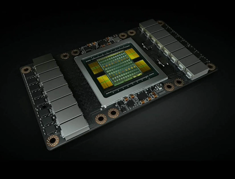
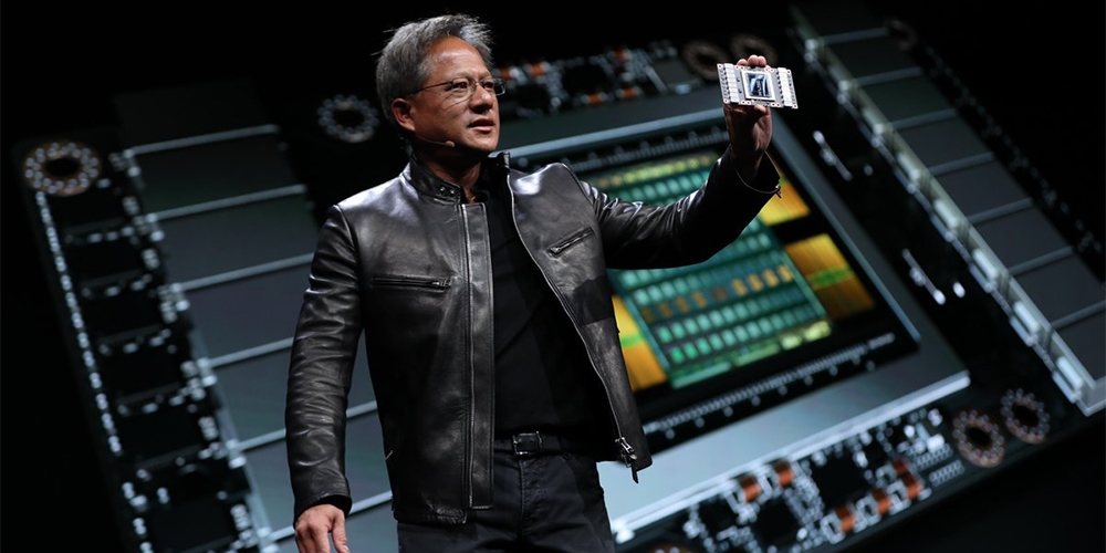
Almost one year after the announcement of the Tesla Pascal P100, NVIDIA has outdone themselves once again and announced the amazing Tesla Volta V100. The new GPU was announced at the 2017 GPU Technology Conference held in San Jose, California. NVIDIA CEO Jen-Hsun Huang made the announcement during the keynote with the claim that the V100 is the most advanced data center GPU ever built. This claim is backed up with $3 billion in research and development costs, huge performance leaps on paper, and proclaimed key compute features for the V100 which include:
The Volta V100 comes with an 815-square millimeter GPU die size compared to the Pascal die size of 610 square millimeters. This pretty much makes the V100 house one of the largest GPU chips ever created. The V100 also comes with the boosted NVIDIA NVLink 2.0 Technology. We previously covered NVLink before and its GPU to CPU connectivity. The basic run down is that NVLink 2.0 provides higher interconnected speed between GPUs, increased number of links, and more scalability compared to the first version of NVLink. According to NVIDIA, NVLink 2.0 will provide speeds up to 300GB/s compared to the 160GB/s that “1.0” provides. An incredible speed increase that is sure to get NVLink users excited.
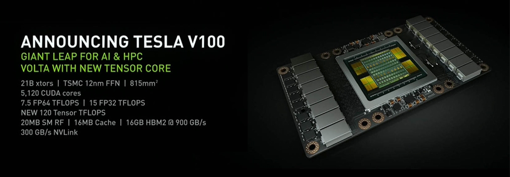
To show how much of a powerhouse the V100 will be let’s compare some numbers. The V100 will contain 21.1 billion transistors, which are something like mini processing cores, compared to the Tesla P100 with 15.3 billion transistors, and the Tesla M40 with 8 billion. The V100 also has up to 5120 usable cores compared to the tesla P100 with 3584 usable cores, that’s a 42% increase! The specification differences can be seen through our comparison chart below:
| Tesla Product | Tesla K40 | Tesla M40 | Tesla P100 | Tesla V100 |
|---|---|---|---|---|
| GPU | GK180 (Kepler) | GM200 (Maxwell) | GP100 (Pascal) | GV100 (Volta) |
| SMs | 15 | 24 | 56 | 80 |
| TPCs | 15 | 24 | 28 | 40 |
| FP32 Cores / SM | 192 | 128 | 64 | 64 |
| FP32 Cores / GPU | 2880 | 3072 | 3584 | 5120 |
| FP64 Cores / SM | 64 | 4 | 32 | 32 |
| FP64 Cores / GPU | 960 | 96 | 1792 | 2560 |
| Tensor Cores / SM | NA | NA | NA | 8 |
| Tensor Cores / GPU | NA | NA | NA | 640 |
| GPU Boost Clock | 810/875 MHz | 1114 MHz | 1480 MHz | 1455 MHz |
| Peak FP32 TFLOP/s* | 5.04 | 6.8 | 10.6 | 15 |
| Peak FP64 TFLOP/s* | 1.68 | .21 | 5.3 | 7.5 |
| Peak Tensor Core TFLOP/s* | NA | NA | NA | 120 |
| Texture Units | 240 | 192 | 224 | 320 |
| Memory Interface | 384-bit GDDR5 | 384-bit GDDR5 | 4096-bit HBM2 | 4096-bit HBM2 |
| Memory Size | Up to 12 GB | Up to 24 GB | 16 GB | 16 GB |
| L2 Cache Size | 1536 KB | 3072 KB | 4096 KB | 6144 KB |
| Shared Memory Size / SM | 16 KB/32 KB/48 KB | 96 KB | 64 KB | Configurable up to 96 KB |
| Register File Size / SM | 256 KB | 256 KB | 256 KB | 256KB |
| Register File Size / GPU | 3840 KB | 6144 KB | 14336 KB | 20480 KB |
| TDP | 235 Watts | 250 Watts | 300 Watts | 300 Watts |
| Transistors | 7.1 billion | 8 billion | 15.3 billion | 21.1 billion |
| GPU Die Size | 551 mm² | 601 mm² | 610 mm² | 815 mm² |
| Manufacturing Process | 28 nm | 28 nm | 16 nm FinFET+ | 12 nm FFN |
To note, this chart is a comparison of prominent NVIDIA Tesla GPUs from the past five years. Based on the numbers alone, it seems NVIDIA's technology is advancing at an incredible speed to match some of today's compute intensive workloads.
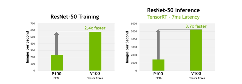
Now you might ask why would anyone need so much power? One of the selling points of the Volta V100 is how it can be used to further increase High Performance Computing (HPC). Specifically, NVIDIA uses Artificial Intelligence (AI) and Deep Learning as a selling point for HPC. Future AI will require systems with large amounts of computational power that can be used to simulate, predict, and analyze, large amounts of data that can be used towards real world applications. The figure below shows how Tesla V100 performance compares to the Tesla P100 for deep learning training and inference using the ResNet-50 deep neural network.
There are many new and improved features that come with the new Volta architecture, but a more in-depth look can wait until the actual release of the GPU. The first batch of Tesla V100 GPUs will first be available inside the new NVIDIA DGX-1 and DGX Station. The DGX-1 will come with eight V100’s and will feature NVIDIA's Deep Learning software stack. The DGX Station will be equipped four V100's interconnected via NVLink and will also feature a liquid cooling system. A slightly less powerful version of the GPU is also planned for released, but there is additional information or estimated cost available yet. The Volta V100 is expected to be released in the third quarter of 2017.
Almost one year after the announcement of the Tesla Pascal P100, NVIDIA has outdone themselves once again and announced the amazing Tesla Volta V100. The new GPU was announced at the 2017 GPU Technology Conference held in San Jose, California. NVIDIA CEO Jen-Hsun Huang made the announcement during the keynote with the claim that the V100 is the most advanced data center GPU ever built. This claim is backed up with $3 billion in research and development costs, huge performance leaps on paper, and proclaimed key compute features for the V100 which include:
The Volta V100 comes with an 815-square millimeter GPU die size compared to the Pascal die size of 610 square millimeters. This pretty much makes the V100 house one of the largest GPU chips ever created. The V100 also comes with the boosted NVIDIA NVLink 2.0 Technology. We previously covered NVLink before and its GPU to CPU connectivity. The basic run down is that NVLink 2.0 provides higher interconnected speed between GPUs, increased number of links, and more scalability compared to the first version of NVLink. According to NVIDIA, NVLink 2.0 will provide speeds up to 300GB/s compared to the 160GB/s that “1.0” provides. An incredible speed increase that is sure to get NVLink users excited.
To show how much of a powerhouse the V100 will be let’s compare some numbers. The V100 will contain 21.1 billion transistors, which are something like mini processing cores, compared to the Tesla P100 with 15.3 billion transistors, and the Tesla M40 with 8 billion. The V100 also has up to 5120 usable cores compared to the tesla P100 with 3584 usable cores, that’s a 42% increase! The specification differences can be seen through our comparison chart below:
| Tesla Product | Tesla K40 | Tesla M40 | Tesla P100 | Tesla V100 |
|---|---|---|---|---|
| GPU | GK180 (Kepler) | GM200 (Maxwell) | GP100 (Pascal) | GV100 (Volta) |
| SMs | 15 | 24 | 56 | 80 |
| TPCs | 15 | 24 | 28 | 40 |
| FP32 Cores / SM | 192 | 128 | 64 | 64 |
| FP32 Cores / GPU | 2880 | 3072 | 3584 | 5120 |
| FP64 Cores / SM | 64 | 4 | 32 | 32 |
| FP64 Cores / GPU | 960 | 96 | 1792 | 2560 |
| Tensor Cores / SM | NA | NA | NA | 8 |
| Tensor Cores / GPU | NA | NA | NA | 640 |
| GPU Boost Clock | 810/875 MHz | 1114 MHz | 1480 MHz | 1455 MHz |
| Peak FP32 TFLOP/s* | 5.04 | 6.8 | 10.6 | 15 |
| Peak FP64 TFLOP/s* | 1.68 | .21 | 5.3 | 7.5 |
| Peak Tensor Core TFLOP/s* | NA | NA | NA | 120 |
| Texture Units | 240 | 192 | 224 | 320 |
| Memory Interface | 384-bit GDDR5 | 384-bit GDDR5 | 4096-bit HBM2 | 4096-bit HBM2 |
| Memory Size | Up to 12 GB | Up to 24 GB | 16 GB | 16 GB |
| L2 Cache Size | 1536 KB | 3072 KB | 4096 KB | 6144 KB |
| Shared Memory Size / SM | 16 KB/32 KB/48 KB | 96 KB | 64 KB | Configurable up to 96 KB |
| Register File Size / SM | 256 KB | 256 KB | 256 KB | 256KB |
| Register File Size / GPU | 3840 KB | 6144 KB | 14336 KB | 20480 KB |
| TDP | 235 Watts | 250 Watts | 300 Watts | 300 Watts |
| Transistors | 7.1 billion | 8 billion | 15.3 billion | 21.1 billion |
| GPU Die Size | 551 mm² | 601 mm² | 610 mm² | 815 mm² |
| Manufacturing Process | 28 nm | 28 nm | 16 nm FinFET+ | 12 nm FFN |
To note, this chart is a comparison of prominent NVIDIA Tesla GPUs from the past five years. Based on the numbers alone, it seems NVIDIA's technology is advancing at an incredible speed to match some of today's compute intensive workloads.
Now you might ask why would anyone need so much power? One of the selling points of the Volta V100 is how it can be used to further increase High Performance Computing (HPC). Specifically, NVIDIA uses Artificial Intelligence (AI) and Deep Learning as a selling point for HPC. Future AI will require systems with large amounts of computational power that can be used to simulate, predict, and analyze, large amounts of data that can be used towards real world applications. The figure below shows how Tesla V100 performance compares to the Tesla P100 for deep learning training and inference using the ResNet-50 deep neural network.
There are many new and improved features that come with the new Volta architecture, but a more in-depth look can wait until the actual release of the GPU. The first batch of Tesla V100 GPUs will first be available inside the new NVIDIA DGX-1 and DGX Station. The DGX-1 will come with eight V100’s and will feature NVIDIA's Deep Learning software stack. The DGX Station will be equipped four V100's interconnected via NVLink and will also feature a liquid cooling system. A slightly less powerful version of the GPU is also planned for released, but there is additional information or estimated cost available yet. The Volta V100 is expected to be released in the third quarter of 2017.